Not your father's Applicard.

 As any old-timer can testify they don't make Applicards like they used to. In fact they don't make Applicards at all! I never had one and a need for a fast z80 card for an Apple 2 computer is not very pressing, but it sure is fun to make a clone using more recent components than the original. I decided to stick to through-the-hole components not as much for a more authentic Apple look, but to make non-professional assembly easy. I only put one surface mount decoupling capacitor on the back of the board because it is very convenient. Here is the prototype board.
card

A did some testing and everything works as it should. At least I can boot CP/M and run all the programs I tried including the Turbo Pascal. The card also works as a RAM disk for DOS 3.3 by loading a driver that came with the PCPI board.

cpm


Now I want no moving parts. PseudoDisk is used as a boot device. In floppy emulation mode.


The 80 column text sure looks good on my VGA thanks to Carte Blanche soon to be offered to the public.

80col


The design is available under a free licence. Do what you want with it, just don't pretend this is your design. If you want  this board, send me an e-mail. I may still have a few PCBs left. Or make your own from my gerbers.

Here is the schematic diagram, the gerber files and the Verilog source of the CPLD.

The design files are here:

CPLD source
schematics
gerbers

Some technical details.

I can't call it an "FAQ list" as nobody asked these questions yet. So here are just the answers.

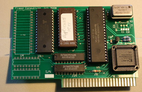
1. 74HCT574 octal flip-flops are used. Can be replaced by LS or  F version, but HC is not good as inputs comes from the Apple system bus - TTL level. HCT is the best as it doesn't take much power and higher speed is not needed.

2. The chip used for clock generation is on the contrary used from the HC series. It produces a much cleaner clock in terms of symmetry than an HCT version.

3. One NAND gate is used to combine A14 and A13 lines to implement a common memory block. The original  card has a jumper to select the 
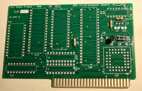
size of the common block - 8K or 16K. By default my card is configured for an 8K size. To reconfigure for a 16K size R8 should be populated and the trace cut between the pads labeled "8/16". You can later install a jumper there to switch between the 8 and 16K.
 
4. U4 and U11 are not normally populated. This is expansion space that I wired for a USB module and a GAL for glue logic. It can be used for some other interface too.

5. Only 2K of the ROM is actually used - the original board had a 2K chip. These days 2716 is rare and pretty slow.
On the other hand 27C512 with 45ns speed (64K) is very inexpensive. 32K is mapped and the other 32K can be switched in instead by pulling pin 1 high. It is wired to the optional GAL. If this is not your idea of fun, just put a zero-ohm resistor as R6, AKA a wire.

6. You can use a quartz crystal or a ceramic rezonator. I like the rezonators because they have the capacitors built-in so C1 and C2 are usually not needed. 

7. I do know that 5V CPLDs are still available. I use 3.3V parts in a 5V design for a reason: the Xilinx 95XL parts are much more robust  than the old 95 series that were very easy to kill with static or by not attaching unused inputs to ground. On this board a number of CPLD pins are connected only to the bus connector. Easy to damage with static when the board is not plugged in. So I opted for a few extra parts - the voltage regulator and 2 resistors but this is compensated by the lower cost of the XL.

This is the production board. First step of assembly.
If you think the holes for DIP pins are too big, I agree. Bigger than was specified in the drill file by 20%. I guess either they had a limited number of drill bit sizes or started celebrating the Chinese New Year early. This is definitely not a problem for hand assembly and I'm not going to complain at the price payed.

board